- 您现在的位置:买卖IC网 > Sheet目录890 > XCL206B333AR-G (Torex Semiconductor Ltd)IC BUCK SYNC 3.3V 0.6A CL-2025
�� �
�
�XCL205/XCL206/XCL207� Series�
�■� OPERATIONAL� DESCRIPTION�
�The� XCL205/XCL/206/XCL207� series� consists� of� a� reference� voltage� source,� ramp� wave� circuit,� error� amplifier,� PWM�
�comparator,� phase� compensation� circuit,� output� voltage� adjustment� resistors,� P-channel� MOSFET� driver� transistor,� N-channel�
�MOSFET� switching� transistor� for� the� synchronous� switch,� current� limiter� circuit,� UVLO� circuit� with� control� IC,� and� an� inductor.�
�(See� the� block� diagram� above.)� Using� the� error� amplifier,� the� voltage� of� the� internal� voltage� reference� source� is� compared� with�
�the� feedback� voltage� from� the� V� OUT� pin� through� split� resistors,� R1� and� R2.� Phase� compensation� is� performed� on� the� resulting�
�error� amplifier� output,� to� input� a� signal� to� the� PWM� comparator� to� determine� the� turn-on� time� during� PWM� operation.� The� PWM�
�comparator� compares,� in� terms� of� voltage� level,� the� signal� from� the� error� amplifier� with� the� ramp� wave� from� the� ramp� wave� circuit,�
�and� delivers� the� resulting� output� to� the� buffer� driver� circuit� to� cause� the� Lx� pin� to� output� a� switching� duty� cycle.� This� process� is�
�continuously� performed� to� ensure� stable� output� voltage.� The� current� feedback� circuit� monitors� the� P-channel� MOS� driver�
�transistor� current� for� each� switching� operation,� and� modulates� the� error� amplifier� output� signal� to� provide� multiple� feedback�
�signals.� This� enables� a� stable� feedback� loop� even� when� a� low� ESR� capacitor� such� as� a� ceramic� capacitor� is� used� ensuring�
�stable� output� voltage.�
�<Reference� Voltage� Source>�
�The� reference� voltage� source� provides� the� reference� voltage� to� ensure� stable� output� voltage� of� the� DC/DC� converter.�
�<Ramp� Wave� Circuit>�
�The� ramp� wave� circuit� determines� switching� frequency.� The� frequency� is� fixed� internally� 3.0MHz.� Clock� pulses� generated� in�
�this� circuit� are� used� to� produce� ramp� waveforms� needed� for� PWM� operation,� and� to� synchronize� all� the� internal� circuits.�
�<Error� Amplifier>�
�The� error� amplifier� is� designed� to� monitor� output� voltage.�
�voltage� divided� by� the� internal� split� resistors,� R1� and� R2.�
�The� amplifier� compares� the� reference� voltage� with� the� feedback�
�When� a� feed� back� voltage� is� lower� than� the� reference� voltage,� the�
�output� voltage� of� the� error� amplifier� is� increased.� The� gain� and� frequency� characteristics� of� the� error� amplifier� output� are� fixed�
�internally� to� deliver� an� optimized� signal� to� the� mixer.�
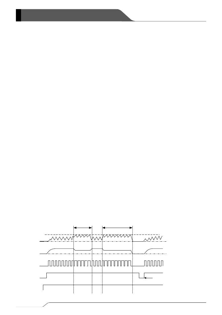
�<Current� Limit>�
�The� current� limiter� circuit� of� the� XCL205/XCL206/XCL207� series� monitors� the� current� flowing� through� the� P-channel� MOS� driver�
�transistor� connected� to� the� Lx� pin,� and� features� a� combination� of� the� current� limit� mode� and� the� operation� suspension� mode.�
�①� When� the� driver� current� is� greater� than� a� specific� level,� the� current� limit� function� operates� to� turn� off� the� pulses� from� the� Lx� pin�
�at� any� given� timing.�
�②� When� the� driver� transistor� is� turned� off,� the� limiter� circuit� is� then� released� from� the� current� limit� detection� state.�
�③� At� the� next� pulse,� the� driver� transistor� is� turned� on.� However,� the� transistor� is� immediately� turned� off� in� the� case� of� an� over�
�current� state.�
�④� When� the� over� current� state� is� eliminated,� the� IC� resumes� its� normal� operation.�
�The� IC� waits� for� the� over� current� state� to� end� by� repeating� the� steps� ①� through� ③� .� If� an� over� current� state� continues� for� a� few�
�milliseconds� and� the� above� three� steps� are� repeatedly� performed,� the� IC� performs� the� function� of� latching� the� OFF� state� of� the�
�driver� transistor,� and� goes� into� operation� suspension� state.� Once� the� IC� is� in� suspension� state,� operations� can� be� resumed� by�
�either� turning� the� IC� off� via� the� CE/MODE� pin,� or� by� restoring� power� to� the� V� IN� pin.� The� suspension� state� does� not� mean� a�
�complete� shutdown,� but� a� state� in� which� pulse� output� is� suspended;� therefore,� the� internal� circuitry� remains� in� operation.� The�
�current� limit� of� the� XCL205/XCL206/XCL207� series� can� be� set� at� 1050mA� at� typical.�
�Depending� on� the� state� of� the� PC� Board,�
�latch� time� may� become� longer� and� latch� operation� may� not� work.�
�placed� as� close� to� the� IC� as� possible.�
�In� order� to� avoid� the� effect� of� noise,� an� input� capacitor� is�
�Limit� <� #� ms�
�Limit� >� #� ms�
�Current� Limit� LEVEL�
�10/25�
�I� Lx�
�V� OUT�
�Lx�
�V� CE�
�V� IN�
�Restart�
�0mA�
�Vss�
�发布紧急采购,3分钟左右您将得到回复。
相关PDF资料
XCL209F083DR
IC STEP DOWN DC/DC 0.8V USP10B03
XHB-00
POWER CHASSIS 600W 6 SLOT
XKC-00
POWER CHASSIS 600W 4 SLOT
XMD-01
POWER CHASSIS 750W 4 SLOT
XNB-01
POWER CHASSIS 400W 4 SLOT
XQC-00
POWER CHASSIS 1200W 6 SLOT
XRC-00
POWER CHASSIS 600W 4 SLOT
XTB-01
POWER CHASSIS 400W 4 SLOT
相关代理商/技术参数
XCL206B333CR-G
功能描述:DC DC CONVERTER 3.3V 制造商:torex semiconductor ltd 系列:XCL206 零件状态:在售 类型:非隔离 PoL 模块 输出数:1 电压 - 输入(最小值):2V 电压 - 输入(最大值):6V 电压 - 输出 1:3.3V 电压 - 输出 2:- 电压 - 输出 3:- 电压 - 输出 4:- 电流 - 输出(最大值):600mA 应用:ITE(商业) 特性:- 工作温度:-40°C ~ 85°C 效率:90% 安装类型:表面贴装 封装/外壳:6-TDFN 裸露焊盘 大小/尺寸:0.10" 长 x 0.08" 宽 x 0.04" 高(2.5mm x 2.0mm x 1.0mm) 标准包装:1
XCL206B333-EVB
制造商:Torex Semiconductor LTD 功能描述:BOARD EVAL SYNC BUCK DCDC 3.3V 制造商:Torex Semiconductor LTD 功能描述:EVAL BOARD, XCL206, DC/DC CONV, 3.3V; Silicon Manufacturer:Torex; Kit Application Type:Data Acquisition; Application Sub Type:Step Down DC / DC Converter; Kit Contents:Board; SVHC:No SVHC (19-Dec-2012); MCU Supported Families:XCL206;
XCL206C103AR-G
制造商:TOREX 制造商全称:Torex Semiconductor 功能描述:Inductor Built-in Step-Down micro DC/DC Converters
XCL206C123AR-G
制造商:TOREX 制造商全称:Torex Semiconductor 功能描述:Inductor Built-in Step-Down micro DC/DC Converters
XCL206C143AR-G
制造商:TOREX 制造商全称:Torex Semiconductor 功能描述:Inductor Built-in Step-Down micro DC/DC Converters
XCL206C153AR-G
制造商:TOREX 制造商全称:Torex Semiconductor 功能描述:Inductor Built-in Step-Down micro DC/DC Converters
XCL206C183AR-G
制造商:TOREX 制造商全称:Torex Semiconductor 功能描述:Inductor Built-in Step-Down micro DC/DC Converters
XCL206C193AR-G
制造商:TOREX 制造商全称:Torex Semiconductor 功能描述:Inductor Built-in Step-Down micro DC/DC Converters